Fig. 5.30: Block diagram of an serial approximative A/D converter
This example represents the ability of Alecsis to support the top-down hierarchical refinement of complex hybrid systems. Fig. 5.30 shows the block diagram of a successive-approximation serial A/D converter. The converter can serve as a mixed signal simulation benchmark for the following reasons:
• the system contains analog (comparator), digital (control and weighting logic, shift register), and mixed-signal subsystems (sample and hold circuit, D/A converter macro model);
• there is a strong feedback loop with logic subsystems present;
• the system is too complex to be simulated at transistor level;
• pure behavioral simulation will not give important details such as possible oscillations or glitches.
Fig. 5.30: Block diagram of an serial approximative A/D converter
The description of the serial A/D converter started with subsystem interface definition. All of the subsystems modules were parametrized in order to handle different output digital word lengths. In the first refinement, all the subsystems (analog, digital and hybrid) were implemented as behavioral to obtain crude results. All of the logic modules were modeled at the Register-Transfer Level, i.e. delay times were identical for all the bits in the register data paths. Transfer characteristic of the analog comparator was modeled using general nonlinear generator and hyperbolic tangens function, while D/A converter and sample and hold circuit employed dual-process strategy similar to the one used for standard D/A domain-coupling modules implicitly inserted by the simulator. The simulation results of the 8-bit configuration with the slow ramp input are shown in Fig. 5.31.
Fig. 5.31: Results of the A/D converter simulation using behavioral representations of the sub-blocks. Digital output variables are at separate plots while analog output variables are all at one plot. Signals data [0] - data[7] represent the output word.
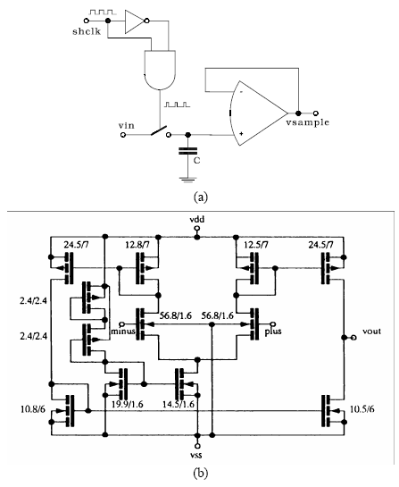
Fig. 5.32:(a) Structural version of sample and hold sub-block used in the second A/D converter partitioning. The circuit consists of logic gates, internally controlled ideal switch, capacitor and operational amplifier described at transistor level.(b) Operational amplifier structure. Transistor channel dimensions are given in µm.
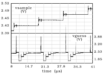
The first simulation was very fast due to the high-level behavioral models. In order to obtain a better accuracy, some of the subsystems were further partitioned into smaller blocks. Digital blocks were modeled at the gate-level, using JK and D-type flip-flops and standard logic gates. The sample and hold circuit was replaced with the circuit shown in the Fig. 5.32(a), with ideal switch, capacitor and a CMOS operational amplifier described at transistor level as shown in Fig. 5.32(b). The same amplifier was used as a comparator. This partitioning helped to detect certain instabilities caused by the small phase margin of the operational amplifier. Another problem occurred due to different delay times of the individual JK flip-flops that form the digital output, resulting in noticeable glitches at the D/A converter output. Both effects are shown in the Fig. 5.33. The second simulation was much slower (455 sec with transistor-level CMOS opamps and logic gates as opposed to 4.7 sec in the case of the behavioral model) primarily because of the analog portion of the system.
Fig. 5.33: Simulation results of the A/D converter with digital circuits at logic level, and analog at transistor level. Attenuated oscillations at the S&H output and glitches at D/A converter output are now clearly visible.